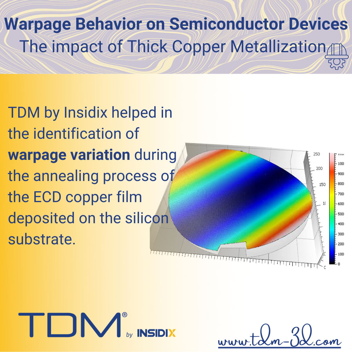
When you wonder how semiconductor devices are manufactured without any deficit or breakage in their fragile and minute composition, it is worthwhile gaining insight into how the “Topography and Deformation Measurement (TDM) ” manufactured by Insidix helped in the identification of warpage variation during the annealing process of the ECD copper film deposited on the silicon substrate. This TDM equipment aided the study carried out by Michele Calabretta and Alessandro Sitta of the STMicroelectronics and Salvatore Massimo Oliveri and Gaetano Sequenzia of the University of Catania on the warpage behavior of semiconductor devices as an impact of thick copper metallization.
Well, the electrochemical deposited, thick film copper acts as an excellent source for electrical and thermal conductivity, and hence, they are considered the building blocks for semiconductors. However, the warpage caused by Cu annealing adversely affects the industrial implementation process of thick copper layers on the silicon substrate, hindering wafer manufacturability. Hence, it is essential to understand the warpage variation to control this impact. And for doing so, the TDM Compact of Insidix comes of great help. Using this device, warpage is experimentally determined at various temperatures considering 2 different annealing profiles.
Experimental Warpage Measurement
Warpage in semiconductors may be defined as the undesired deformation of the wafer that is caused due to stress occurring from thermal treatments. Thus, TDM Compact helps quantify this warpage behavior using a Projection Moiré phase-shift method. The said commercial equipment from Insidix consists of two main components, namely:
- Projection system – It projects the strip patterns piloted by the software
- Viewing system – It consists of a CCD camera and optics whose grating is phase-shifted against the projection to acquire a 3D reconstruction.
So, after the sample is illuminated with a stripe pattern, its images are captured by the TDM camera at different temperature profiles during both the heating and cooling phase. After that, the warpage-temperature behavior is automatically plotted and analyzed by TDM.
However, the warpage behavior showcases a change in the slope during the heating phase at 150℃, indicating that the warpage reached its maximum limit. This observation can correspond to an irreversible warpage behavior in the copper layer, which needs further physical analysis for better understanding.
Physical Analysis
So, as the next step, differential scanning calorimetry (DSC) analysis is used to monitor the occurrence of thermally driven phenomena in the copper layer during the heating cycle. It was found that an exothermic event got initiated at 160℃.
So, for in-depth analysis, some samples are cross-sectioned by the Focused Ion beam technique and analyzed with Scanning Electron Microscopy. Then, the observations are compared with the warpage map generated from Insidix’s TDM. The comparative study highlights that at temperatures of 150° and 250°, respectively, there has been an increase in the grain size between the samples.
Thus, it is evident that the experimental measurements obtained using Insidix are similar to the DSC analysis results. Also, this observation elucidates the warpage behavior of the copper layer in terms of residual warpage after the thermal process, and slope modification in the warpage map is measured at 150℃.
Finite Element Model (FEM) for Warpage Calculation
This study uses two analytical approaches to predict the stress and warpage in the wafer. One of them is Stoney’s equation, which is used as a reference to measure the thermal warpage in the film. However, this equation applies to homogenous materials and shows linear elastic behavior; hence, it is unreliable during the entire annealing process due to copper’s non-linear behavior.
The second most used approach is the Timoshenko formulation, which calculates the stress in bi-material thermistors. The thermal inputs of this formulation are converted into a set of equivalent forces and momentum, used for 3+ materials.
So, based on these two literature approaches, the Finite Element Model is developed, along with Comsol Multiphysics, to calculate the warpage variation and mechanical stress due to varying temperatures. It is a customized 3D model that analyzes linear elastic warpage and stress behavior.
After that, a comparison of the warpage-stress behavior between the FEM model, experimental warpage measurement, and physical analysis results is performed. It is noticed that the FEM warpage shows a close resemblance to the results obtained in experimental warpage measurements. Thus, it validates the efficiency of Insidix’s TDM Compact device.
Conclusion
The study primarily describes the evolution of the deformation during the annealing process of ECD copper film at various degrees of temperature. And in the process, TDM has played a significant role in measuring the warpage and stress factors of the semiconductor device.
The accordance and agreement between the results obtained in the warpage map produced by the TDM equipment, DSC-based physical analysis, and Finite Element Model (FEM) assure the efficiency of Insidix’s TDM. Also, it showcases the importance of Topography and deformation measurement (TDM) in the impact of copper metallization.
Visit MDPI website to download the paper: https://www.mdpi.com/2076-3417/11/11/5140